
Crosstalk: two pairs that were both fine on their own
Each high speed pair was tested by itself with protection fitted. Both met their eye mask with margin and the ESD qualification passed on every pin. Run both pairs at the same time and one of them starts showing bit errors. Nothing is damaged, nothing runs hot, and the link comes back on a retrain.
The case: two pairs that were clean on their own
Two high speed pairs on the same connector, each with a low capacitance protection array fitted. Each pair was brought up and tested on its own. Both met their eye mask with margin. The ESD qualification passed on every pin.
Then both pairs were run at the same time, and one of them started showing bit errors.
The important detail is what did not happen. Nothing was damaged. Nothing ran hot. Nothing needed replacing, and the link came back by itself on a retrain. A part that has been destroyed does not recover on a retrain.
This is a signal problem, not a protection failure
It is worth separating these two early, because they get investigated as one thing and they are fixed in completely different places.
- An ESD problem is fixed by the device. You change the part, or you change where it sits relative to the connector, and the clamping behaviour changes.
- A crosstalk problem is fixed by geometry. The device only helps or hurts by where its pins sit, and no amount of changing its clamping specification will move the answer.
So the question to answer is not "is the protection good enough". It is: is the protection on these lines carrying one pair into the other, and if so, how much noise does that actually put on the quiet pair?
What crosstalk is
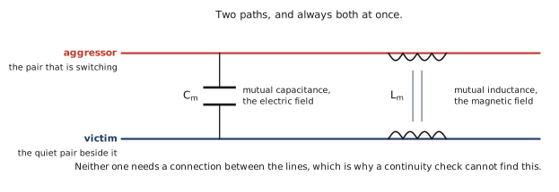
A line that is switching pushes energy onto the quiet line beside it. There are two paths and they are always both present.
- The electric field couples through the mutual capacitance. The two conductors form a small capacitor, and a changing voltage on one drives current into the other.
- The magnetic field couples through the mutual inductance. Changing current on one line links flux into the loop of the other and induces a voltage in it.
Neither path needs a connection between the lines. That is worth saying out loud because it explains why this survives every check that looks for one. A continuity test, a netlist review and a visual inspection will all pass. There is nothing there to find, and the coupling is still happening.
How much couples, and why it gets worse every generation
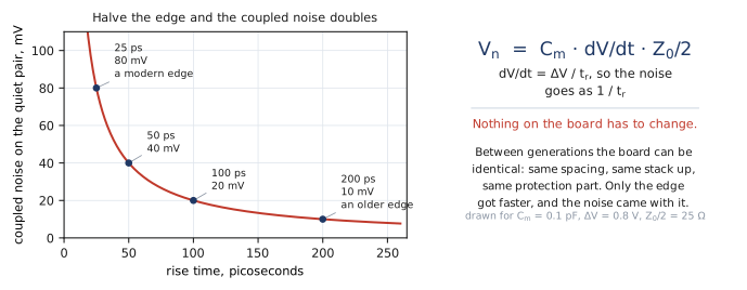
One equation carries most of it. For the capacitive path, the noise on the quiet line is:
Vn = Cm × dV/dt × Z0/2
The rate of change of voltage is the swing divided by the rise time, so the coupled noise goes as one over the rise time. Halve the edge and the coupled noise doubles.
This is why the same board gets worse from one product generation to the next while nothing visible about it has changed. Same spacing, same stack up, same protection part, same everything. The only thing that changed is the edge, and the noise came with it. A design that had comfortable margin at a 200 ps edge has a quarter of that margin at 50 ps.
It also explains the shape of this case. Each pair alone is fine because there is no aggressor. The moment both run, one becomes the aggressor for the other.
Where the protection part comes into this
A protection device does two entirely separate things to a high speed line, and they are constantly blamed for each other.
- It adds capacitance to the line. Every protection device is a capacitor sitting across the signal. That is loading. It shows up as insertion loss and a slower edge, on that line only.
- Its pins set how close the pairs run. The package decides how close the two pairs have to pass each other, and whether anything sits between them. That is coupling. It shows up as noise on the other pair.
These have different causes and different fixes. Lower capacitance fixes loading. It does nothing at all for coupling. Only geometry fixes coupling.
Which leads to the sentence worth taking away from this note: if you compare protection parts on capacitance alone, you have compared half of it.
Effect one, loading: what the capacitance costs
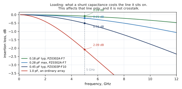
A shunt capacitor on a transmission line has a straightforward insertion loss, and the numbers at 5 GHz are worth knowing because they are smaller than people expect at the low end and larger than people expect at the high end.
- 0.18 pF costs about 0.09 dB
- 0.28 pF costs about 0.21 dB
- 0.45 pF costs about 0.51 dB
- 1.0 pF costs about 2.09 dB
Two things fall out of that list. The first is that going from 0.45 pF to 1 pF is not a small step: it is four times the loss, not twice, because the loss climbs faster than the capacitance does. The second is that at the low end the differences are genuinely small, so a part at 0.18 pF against one at 0.28 pF is a fraction of a tenth of a decibel and is almost never what is costing you the margin.
This model is not a guess. It predicts 0.51 dB at 5 GHz for 0.45 pF, and that is the figure we measure on a real 12 Gbps link and publish in the PZ0303P-F10 datasheet.
Effect two, geometry: where the ground pins sit
Coupling inside a pair is the pair. That is what a differential pair is for and it is not a problem. Coupling between pairs is the problem, and the protection part sits at exactly the point where the two pairs are forced closest together.
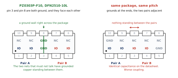
The PZ0303P-F10 is a ten pin DFN2510-10L. Along the bottom row the order is channel 1, channel 2, ground, channel 3, channel 4, so pin 3 sits directly between Pair A and Pair B.
The part that matters more is on the other side. The top row runs 10, 9, 8, 7, 6, and pin 8 is also a ground, directly opposite pin 3. So this is not a single grounded pin between the pairs. It is a ground on both rows at the same position, which makes a wall of grounded copper straight across the package at exactly the point where the two pairs pass each other.
That is where a ground pin genuinely earns its place, because it stands between the two nets that must not talk to each other and gives the coupled field somewhere to terminate instead of continuing into the neighbour.
Now look at a part with the same pin count and the same pitch, but the grounds at the end and the two pairs adjacent. It has an identical capacitance on the datasheet and it will sort identically in a parametric search. It is a worse part for this job and nothing in the specification table says so.
What we would fit
- PZ0303P-F10 where there are two pairs. Four channels, so both pairs go into one part, with grounded pins on both rows between them. 0.45 pF, 3.3 V working, 6.0 A at 8/20 µs, dynamic resistance 0.21 ohms, ±16 kV contact and ±21 kV air, DFN2510-10L.
- PZ0302A-F7 where there is a single pair and capacitance is the tightest number on the page. Two channels at 0.18 pF typical and 0.28 pF maximum, 3.3 V working, 6.5 A, ±18 kV contact and ±21 kV air, DFN1610-6L.
One thing about how we write those numbers. We publish a maximum capacitance, not only a typical. A typical figure is the middle of a distribution and your worst boards are not built from typical parts. Design to the maximum, and if a competing datasheet only gives you a typical, that is worth asking about before you compare the two.
What we need from you to answer this properly
Both effects can be put on paper before the board is laid out, but only one of them is on the datasheet. The capacitance we already know. The coupling depends on your geometry, so it needs four things:
- The line rate, which sets where on the insertion loss curve you are sitting.
- The edge rate, which is the one that actually drives the coupling and is usually faster than the line rate implies.
- The pair pitch, meaning how far apart the two pairs run and for how long they run in parallel.
- The stack up, because how close the reference plane sits decides how much of the field stays local instead of reaching the neighbour.
With those four we can give you the loading and the coupling as numbers rather than as opinions, and tell you which of the two is actually costing you the margin. Quite often it is not the one being blamed.
The short version
- Two pairs that are each clean alone and fail together is crosstalk, not a protection failure. Nothing is damaged and the link recovers on a retrain.
- Crosstalk couples through mutual capacitance and mutual inductance, and neither needs a connection, so a continuity check will never find it.
- Coupled noise goes as one over the rise time. Halve the edge and it doubles, with nothing on the board changing.
- A protection part does two separate things: its capacitance loads the line it sits on, and its pin order sets how much the pairs couple to each other.
- Lower capacitance fixes loading and does nothing for coupling. Only geometry fixes coupling.
- At 5 GHz, 0.45 pF costs about 0.51 dB and 1 pF costs about 2.09 dB, which is four times the loss and not twice.
- On the PZ0303P-F10, pin 3 and pin 8 are both grounds and they face each other, so a ground wall runs right across the package between the two pairs. Pitch does not tell you that, only the pin order does.
- Design to the maximum capacitance, not the typical.