
USB-C Power Delivery (PD 3.1)
Everything Magnias makes for a USB-C fast-charging port, from the wall charger to the device, 20 W to 240 W.

What is USB-C Power Delivery?
USB-C Power Delivery (USB PD) is the fast-charging standard behind modern USB-C. One reversible cable carries both data and power, and the two ends negotiate the right voltage automatically, from 5 V up to 48 V, and up to 240 W. It's what lets a single charger top up a phone, a laptop, or even a power tool.
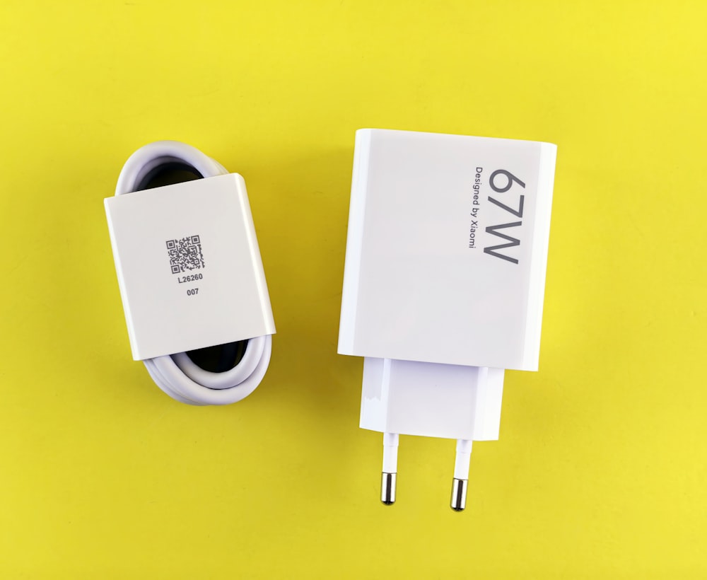
You'll find USB-C PD in phone & laptop chargers, power banks, monitors, docks and hubs.
Where Magnias fits in the port
Magnias makes the semiconductors around the USB-C connector, the power switches that turn VBUS on and off safely, and the protection that shields the port from surges, static and faults. Every colored block below is a part we supply.
For the design engineer
How the parts are chosen, the topology, and the device per role at each power class.
The MOSFET roles, and why they come in pairs
USB-C VBUS carries current in BOTH directions, source and sink swap roles (plus OTG and fast-role-swap). A single MOSFET blocks voltage one way, but its body diode conducts the other. So every PD VBUS path uses two N-channel MOSFETs source-to-source: one blocks forward, one blocks reverse. That is why the power-tier table lists the VBUS B2B parts as pairs (×2).
N-MOS vs P-MOS, which to use
| N-MOS | P-MOS | |
|---|---|---|
| RDS(on) & cost | Lower (2–3×), widest lineup | Higher, narrower lineup |
| High-side gate drive | Needs charge pump | Simple pull-down, none needed |
| Best fit | Efficiency + high current (with a PD IC) | Discrete BOM, default-OFF safe |
Five discrete-FET roles in one PD port
VDS rule of thumb. VBUS path: 30 V class at 5 / 9 V, 40 to 60 V class up to 20 V (SPR), 100 V class or higher at EPR 28 V and 48 V. SR side: 60 to 100 V for SPR, 120 to 150 V for EPR.
PD charger reference circuit
MOSFETs by power tier
One device per role, 20 W → 240 W, every P/N verified in-production.
| Tier | VBUS B2B | Load / Protect | HV Switch | Sync Rect |
|---|---|---|---|---|
| 20–30 WSPR 5 / 9 V | PMS9R5D03BQ | PMS0314AQ | PMH65N510GF | PMS0602AG |
| 45–65 WSPR 15 / 20 V | PMS11R5D06HQ | PMS0401DG | PMH65N340CF | PMS3N10EG |
| 100 WSPR 20 V × 5 A | PMS1R2N06TG ×2 | PMS0401DG | PMH65N270AF | PMS3N10EG |
| 140 WEPR 28 V | PMS1012AQ ×2 | PMS1012AQ | PMH65N270AF | PMS6R5N12AG |
| 240 WEPR 48 V | PMS3R9N15HL8 ×2 | PMS1012AQ | PMH65N130DF | PMS3R9N15HL8 |
VDS carries EPR transient headroom. Up to 65 W the VBUS back-to-back pair is one dual N+N MOSFET (PDFN3333-8L). From 100 W up it is two single low-RDS(on) N-MOSFETs in series (×2). At 240 W the same 150 V part (PMS3R9N15HL8) serves the VBUS pair and the SR.
PD sink switch, one part for the whole sink ring
On the device (sink) side, the PD sink switch is the high-side switch that connects USB-C VBUS to the system rail once PD negotiation completes. It integrates the power FET plus the protection you would otherwise build from a discrete back-to-back FET, a controller, and a sense network:
Completes the PD BOM
Beyond the MOSFETs and protection, a full PD design pulls in these, all from Magnias:
Typical PD designs
Core PD parts
AEC-Q101 (-A) versions exist for many MOSFET, TVS and ESD parts. Magnias parts are halogen-free and RoHS compliant as standard.
Designing a USB-C PD port? Get the full BOM.
Tell us the power class and whether the port is source, sink or bidirectional: our FAE team replies within one business day with the back-to-back pair, HV / SR MOSFETs, sink switch and ESD / TVS for your design, plus sample availability.