OSFP Optical Module Support ICs
Voltage conversion, power switching, and supervision ICs for 400G, 800G, and 1.6T OSFP transceivers.
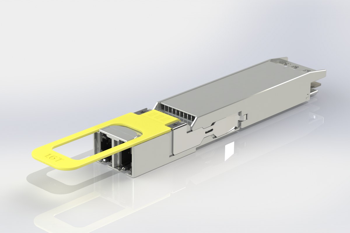
OSFP (Octal Small Form-factor Pluggable) is the dominant pluggable optical module form factor for AI-cluster and hyperscale switch interconnect. Each module needs a small but precise set of support ICs — multi-voltage conversion, hot-plug load switching, rail supervision, and signal level shifting — that sit alongside the optical engine and DSP. Magnias provides a complete BOM of LDOs, buck converters, load switches, comparators, and logic for the support circuit, scaling cleanly from 400G to 1.6T module power budgets. The same BOM also supports Linear Pluggable Optics (LPO/LRO) variants, which remove the DSP and can cut module power by up to 40–50% depending on architecture — only the core-supply current ratings change.
What an OSFP module needs from its support circuit
Each line below names a system-level need and the IC class that addresses it. The same set scales from 400G to 1.6T — only the current ratings change.
| System-level need | IC class that addresses it |
|---|---|
| Multi-voltage DC conversion | LDO + Buck |
| Low-IQ analog bias rails | Low-quiescent-current LDO |
| Sub-1 V efficient core supply | Buck with BIAS pin |
| Hot-plug inrush limiting | Load switch (controlled slew) |
| Independent rail sequencing | Two load switches |
| Output discharge on shutdown | Load switch with RPD |
| Voltage supervision / POR | Dual comparator |
| Wire-OR interrupt drive | Open-drain buffer |
| Host CMOS to chipset signal bridge (CMIS 5.x two-wire management bus) | Level-shifter buffer (push-pull) |
Three circuit groups inside every OSFP module
The Magnias OSFP BOM splits into three functional groups. Each group has one or more positioned Magnias parts and a benchmark from a competitor for comparison.
Three Magnias parts cover the OSFP voltage tree — fixed photodiode-bias LDO, low-IQ analog bias LDO, and a high-efficiency buck for sub-1V core rails.
Magnias load switches gate the 3.3V rails, a dual comparator monitors rail validity for the host, and an open-drain buffer drives the wire-OR interrupt line.
Push-pull level-shifter buffer (2-channel × 2 instances) translates the 3.3V host CMOS signals — including the CMIS 5.x two-wire management bus to the internal MCU — into the 1.8V chipset domain. Magnias MI2129B-F14.
OSFP support-circuit block diagram
Choose a data rate to see the support circuit. The topology is shared across 400G / 800G / 1.6T — only the current ratings differ. Click (or tap) any blue block for the recommended Magnias part. Note: rail names (PD2V5, DVDDM1, 3V3_1, 3V3_2) are representative — actual labels vary by DSP / TIA / driver vendor.
1.6T OSFP targets next-gen AI cluster interconnect. The support circuit retains the same blocks but with the highest current ratings — the buck's 2A rating on MI2262G-F15 and the load switch's 12A continuous rating on PSW1510-A10 are key headroom margins for this segment. Note: today's 1.6T pluggable OSFP modules (8 × 200G lanes, same cage as 800G) typically operate at ~20–25 W. OSFP-XD is a separate, non-backward-compatible 16-lane form factor that extends the thermal envelope up to ~30 W.
Magnias parts vs benchmark — side-by-side
Each row compares the Magnias-positioned part to a competitor benchmark on key parameters. The Magnias edge column highlights where the Magnias part wins.
Group 1· Voltage Conversion
| Parameter | Magnias | Competitor |
|---|---|---|
| V_IN | 2.5 – 6 V | 1.4 – 5.5 V |
| V_OUT | 2.5 V fixed | 2.5 V fixed |
| I_OUT max | 300 mA | 150 mA |
| I_Q | 500 nA | 50 µA |
| Dropout | 500 mV / 300 mA | 230 mV / 150 mA |
| PSRR @ 1 kHz | 60 dB | 65 dB |
| Package | TDFN1010-4L | SON-6 |
| Parameter | Magnias | Competitor |
|---|---|---|
| V_IN | 1.2 – 5.5 V | 1.6 – 6.0 V |
| V_OUT | 3.3 V fixed / ADJ | 4.0 V |
| I_OUT max | 350 mA | 300 mA |
| I_Q | 1.3 µA | 6.5 µA |
| PSRR @ 1 kHz | 80 dB | 95 dB |
| Parameter | Magnias | Competitor |
|---|---|---|
| V_IN | 2.55 – 6 V | ≥ 3 V |
| V_OUT | 0.6 – 6 V adjustable | 0.72 V FB-set |
| V_REF | 0.6 V ± 1% | ≈ 0.5 V |
| I_OUT max | 2 A | ~1 A |
| f_SW | 1.6 MHz | — |
| Efficiency | Up to 95% | — |
| Package | DFN1510-6L | WCSP |
Group 2· Power Switching & Supervision
| Parameter | Magnias | Competitor |
|---|---|---|
| V_IN | 0.1 – 5.5 V | 0.5 – 13.5 V |
| I_OUT continuous | 12 A | 10.5 A |
| R_ON typ | 3.2 mΩ | 12.8 mΩ |
| Soft-start | Programmable slew | Fixed |
| Discharge | Integrated | Integrated |
| Package | AQFN 1.5 × 2.0 mm | DFN-8 5 × 5 mm |
| Parameter | Magnias | Competitor |
|---|---|---|
| Supply | 1.2 – 5.5 V | 1.6 – 6.5 V |
| Output | Push-pull | Push-pull |
| Channels | 2 (dual) | 2 (dual) |
| Input CM | Rail-to-rail | Rail-to-rail |
| t_pd | 300 ns @ 100 mV | 3 µs typ |
| Hysteresis | Built-in | Built-in |
| Package | AQFN 1.5 × 1.5 mm | SC-70-8 |
| Parameter | Magnias | Competitor |
|---|---|---|
| V_CC | 1.65 – 5.5 V | 1.65 – 5.5 V |
| V_I tolerance | 0 – 5.5 V | 0 – 5.5 V |
| V_O off | 0 – 5.5 V | 0 – 5.5 V |
| I_OL drive | 24 mA | 24 mA |
| t_pd max | 3.7 ns | ~5 ns |
| Channels | 2 (use 1) | 1 |
Group 3· Voltage Domain Crossing (Roadmap)
Magnias OSFP BOM summary
| Function | Magnias P/N | Package | Applies to | Notes |
|---|---|---|---|---|
| Photodiode bias LDO | PR9030-2V5TF11 | TDFN1010-4L | All rates· rail PD2V5 | 300 mA, 500 nA IQ. 100× lower IQ than competitor benchmark. |
| Analog Bias LDO (3.3 V fixed or ADJ) | PSR9031-3V3TF11 | TDFN1010-4L | All rates· analog bias rails | 350 mA, 1.3 µA IQ — 5× lower than competitor. PSR9031-3V3TF11 fixed for 3.3 V analog rails; PSR9031-ADS5 adjustable for custom analog voltages. |
| Synchronous Buck (DSP core) | MI2262G-F15 | DFN1510-6L | All rates· DSP core rail DVDDM1 | 2 A, 1.6 MHz, up to 95% efficient. Drop-in for FB-set 0.72V. |
| 3V3 Hot-Plug Load Switch (main, 12A class) | PSW1510-A10 | AQFN 1.5×2.0 mm-10L | All rates· two instances (3V3_1 / 3V3_2) | 12 A continuous, 3.2 mΩ R_ON typ (6 mΩ max). Wide VIN 0.1–5.5V. Programmable slew rate + integrated discharge. |
| 3V3 Hot-Plug Load Switch (alt) | PSW5192D-C11 | DFN | All rates· same position | Alternative load switch with 65 Ω discharge and verified soft-start. |
| Dual Comparator / Supervisor | MVC1362-AC | AQFN 1.5 × 1.5 mm | All rates· LPWn / RSTn (OSFP MSA) | 300 ns t_pd, push-pull, rail-to-rail. 10× faster than competitor. |
| Open-Drain Buffer (wire-OR) | ML74LVC2G07-TW | SOT-563 | All rates· INT line (OSFP MSA) | Dual-channel, 24 mA I_OL, 5.5V tolerant. 3.7 ns t_pd max. |
| Level Shifter · 2-bit bidirectional × 2 instances | MI2129B-F14 | DFN1410-8L | All rates · CMIS / I2C bus bridge to chipset | Push-pull · 24 Mbps · 7.1 ns t_pd. Use 2 instances for 4 channels covering the CMIS / I2C management bus from host CMOS into chipset domain. |
Request samples or an OSFP design review
Designing a 400G, 800G, or 1.6T OSFP module? Need samples of the LDO / buck / load-switch / comparator parts above, or want our FAE team to review the support-circuit BOM against your DSP and optical engine? Tell us the data rate and the parts of interest — we reply within one business day.