
Damage that builds up: the failure with no event attached to it
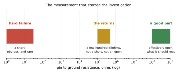
Full IEC 61000-4-2 qualification, every level, every pin, criteria A throughout. The product shipped. Months later units come back with the interface pin reading a few hundred kilohms to ground, and nobody can name a single thing that happened to them. No drop, no strike, no complaint about handling. They simply stopped.
What shipped
An ordinary product with an ordinary external interface. It went through full IEC 61000-4-2 qualification: every level up to the requirement, every exposed pin, criteria A throughout. There was nothing marginal about the result and nothing unusual about the design.
Then it shipped, and for a while nothing happened.
What came back
Units returning with the interface pin reading a few hundred kilohms to ground where it should read open. Not a short and not an open. Something in between, which is the reading nobody has a category for.
What made it worse is that the failures had no event attached to them. No drop. No reported static shock. No complaint about handling. The units simply stopped working, and the field could not tell anyone why, because from the field's point of view nothing had occurred.
Why it was hard to pin down
Two facts blocked every obvious line of investigation.
- The same board, retested with an ESD gun, still passed. So the design was not marginal against the standard, and the qualification result was not a fluke.
- The damaged units and the good units came off the same reel on the same day. So it was not a lot problem, not a process excursion, and not a supplier change.
Put those together and the usual conclusions are all unavailable. It is not the design, not the lot, and not a single identifiable event. That combination is the signature of this failure mode, and it points at something the tests were never asking about.
The industry already has a name for the parts this produces. They are called walking wounded: devices degraded by a stress that was not strong enough to destroy them, and carrying that damage forward into the field.
The mechanism: damage accumulates before anything breaks
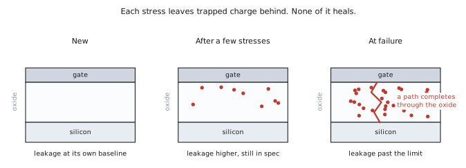
A discharge that is well inside what a device can survive still puts hot carriers through its oxide. Some of those carriers get trapped, and trapped charge stays where it is. The device works afterwards, and it is not the same device it was before.
Run that again and the traps add up. Leakage rises a little with each one. Nothing about this is dramatic and nothing about it is visible from outside, until enough traps exist that a conducting path completes through the oxide, and then the part fails.
The important consequence is in the word accumulates. The stress that kills the part is not special. It is very often the smallest one, arriving last, on a device that had already used up its margin. That is why the failure has no event attached to it: the event that mattered was not the one that finished it.
Which device is degrading, the chip or the protection part
This question decides what you measure, so it is worth being exact rather than talking about "the device". Both of them accumulate damage, and they do it by different mechanisms.
- The IC behind the port degrades in its gate oxide. That is the mechanism drawn in the figure above: hot carriers, trapped charge, and eventually a path through the oxide. It is a dielectric failure, and it is why the classic symptom is an input pin that has stopped being an open circuit.
- The protection device degrades in its junction. Each event puts current through a small area of silicon, and repeated events leave localised damage behind. It is a thermal and structural failure rather than a dielectric one, and it shows up as rising reverse leakage on the array itself.
The two are connected, which is the useful part. A clamp with more margin turns on harder and earlier relative to the stress, so less of every event reaches the IC. Buying margin on the protection part is not only about keeping the protection part alive. It is mostly about keeping the chip behind it out of the region where its oxide starts collecting charge.
So when you go measuring, be clear about which one you are probing. Leakage on the protection array tells you the array has been working hard. Leakage or a resistance reading on the IC pin tells you the stress got past it. Both are useful, and they mean different things.
Why every test you run still passes
This is the part that frustrates people, because the tests are not wrong. They are answering different questions from the one you need answered.
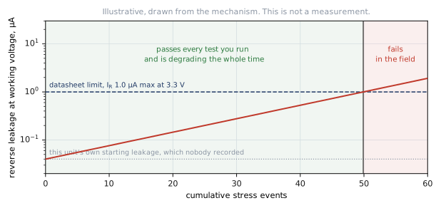
- A functional test asks whether the part works. It does. A device with a damaged oxide and elevated leakage still passes functionally, right up until it does not.
- A leakage test asks whether the part is inside its datasheet limit. It is. For the PZ0303P-F10 that limit is IR 1.0 µA maximum at VRWM 3.3 V, and a degrading part sits under it for almost the entire process.
- Re-running the ESD gun asks whether the design survives the standard. It does, which is exactly what the qualification already told you.
So every instrument in the building says the part is fine, and every one of them is telling the truth.
The baseline nobody keeps
The damage is real and it is measurable the whole time. It is just not measurable against the number on the datasheet. It is only visible against that individual unit's own starting leakage, and almost nobody records that.
A part that began at 40 nA and now sits at 400 nA has degraded by a factor of ten and is still comfortably inside a 1 µA limit. Every incoming inspection in the world passes it. The only measurement that would have caught it is one taken before the stress and compared afterwards, on the same device.
By the time the number crosses the limit printed on the page, the failure is not in your lab. It is in the field, and it was in the field for some time before anybody booked the return.
What we publish, and why we publish it that way
We state an absolute rating on every ESD part rather than a statement that it passed at somebody's required level. Those two look similar on a page and they are not the same claim.
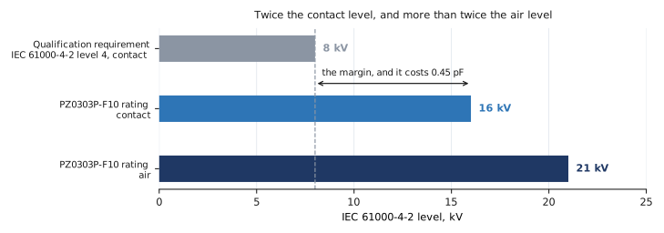
"Passes 8 kV" tells you the device survived the test you had to run. It tells you nothing about where the device begins to degrade, and degradation begins well before destruction. An absolute rating tells you where the part actually stops, and the useful number is the distance between that and your requirement. The margin is what predicts your return rate.
A note on what this claim covers, since it matters: across our ESD line the absolute contact and air ratings are stated on every datasheet. Dynamic resistance, which sets how much voltage the IC behind the part actually sees, is stated on many of them but not yet on all. Where you need it and it is not printed, ask us and we will send it.
Buy the margin, it is the cheapest fix available
Every other fix for this failure mode is expensive. Tightening handling controls across a supply chain is expensive. Adding incoming leakage screening with a per unit baseline is expensive. Redesigning a port after returns have started is very expensive.
Specifying a part that starts degrading a long way above your requirement costs, in the case above, 0.45 pF.
- High speed ports. PZ0303P-F10, 16 kV contact and 21 kV air against an 8 kV requirement, at 0.45 pF and 4 channels. The margin costs essentially nothing in signal integrity, which is the whole reason it is worth buying here.
- General purpose lines. The PS and PT families. Capacitance is less binding, so take the headroom where it is available rather than matching the requirement exactly.
- Anywhere the port is user accessible. This is where cumulative stress actually happens, because the number of small events over a product's life is large and none of them get reported.
The instinct to specify a part that exactly meets the requirement is a reasonable instinct in most of engineering. Here it puts the start of degradation right next to where the product lives.
If you already have returns and no reproducible event
There is a measurement that usually separates the two populations, and it costs nothing.
- Measure leakage, not function. Function is what is hiding the problem. Leakage is where latent damage shows up first.
- Probe both devices, and keep them separate. On the protection array, measure reverse leakage from the I/O pin to ground at the working voltage, which for a 3.3 V part means IR at 3.3 V. On the IC, measure pin to ground resistance with the part unpowered, which is the reading that produced the few hundred kilohms above. They answer different questions and you want both.
- Compare returned units against new stock of the same part number. You have no per unit baseline, so use the population as the baseline instead. A clear separation between the two groups is the answer.
- Do it at the working voltage, not at breakdown. This failure lives in the leakage region, not at the knee.
If the returned units sit an order of magnitude above new stock while both remain inside the datasheet limit, you have found it, and no ESD gun was going to reproduce it for you. If the array looks clean and the IC pin does not, the stress went past the protection rather than into it, and that points at the margin rather than at the part's own endurance.
The short version
- A failure with no event attached to it, on units from the same reel as the good ones, is the signature of cumulative damage rather than a single strike.
- Stress below the destruction level still traps charge in the oxide, and trapped charge does not heal. The part that fails is the one that had already spent its margin.
- Both devices age, by different mechanisms. The IC degrades in its gate oxide, the protection array degrades in its junction. Measure them separately, because they mean different things.
- Functional tests and datasheet leakage limits both pass throughout the degradation. They are answering a different question.
- The damage is only visible against the unit’s own starting leakage, which almost nobody records.
- A pass at your required level is not the same claim as an absolute rating. The distance between the two is what predicts the return rate.
- With returns and no reproducible event, compare reverse leakage at working voltage between returned units and new stock.