
Latch-up: the protection device that never turned off
The board passes every functional test. Then it goes through ESD testing, and one port stops working. The protection device is warm. Replace it, power-cycle, and the board is fine again, until the next discharge. The part is not too weak. It is still switched on.
What was being built
A USB Type-C port on a 5 V rail. Ordinary design: connector, ESD protection on the data lines and on VBUS, then the controller behind it. The engineer chose the protection part the way most people do, by looking for the lowest clamping voltage on the datasheet. Lower clamping means less voltage reaching the chip, so lower must be safer.
What actually happened
During the ±8 kV contact discharge test, the port stopped responding. Measured on the bench afterwards:
- VBUS sitting at about 2.4 V instead of 5 V
- Current into the protection device far above its normal leakage, milliamps rather than nanoamps
- The device noticeably warm to the touch
- A power cycle brought everything back to normal
That last point is the important one. A destroyed component does not recover when you remove and reapply power. This device was not damaged. It was conducting, and it had been conducting since the discharge, long after the discharge itself was over.
The answer everyone reaches for first
The obvious reading is "the transient was bigger than the part could take, so use a stronger part." That leads to choosing a device with a higher surge rating, which is usually a bigger die, which usually means higher capacitance. On a USB 3.x lane that capacitance costs signal integrity, so now the design has two problems instead of one.
And it does not fix anything, because nothing was overloaded. To see what really happened you have to look at how the device behaves while it is turning on, and the only measurement that shows that is a TLP curve.
The measurement that shows the problem
TLP (Transmission Line Pulse) testing fires a short, precisely controlled pulse at the device and records the voltage across it and the current through it. Repeat at increasing levels and you get the device's real current–voltage curve, not the marketing number, the actual behaviour.
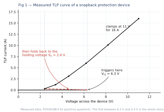
Read it from left to right:
- From 0 V up to 6.3 V the device is off. Almost no current. This is the trigger voltage, usually written Vt1.
- At 6.3 V it switches on, and the voltage across it drops backwards to about 2.4 V. That is the fold, and this device type is named after it: snapback.
- From there it conducts, rising to 11 V at 16 A. That low voltage while conducting is exactly why snapback devices give such good clamping numbers.
The number that matters is the one at the bottom of the fold: the holding voltage, Vh. It is the voltage below which the device lets go. Above it, the device keeps conducting.
Why it never turned off
The discharge triggered the device. Fine, that is its job. The problem is what the device saw immediately afterwards.
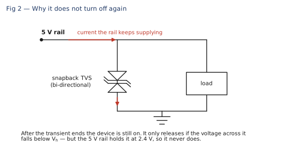
The device sits across a live 5 V rail. Its holding voltage is 2.4 V. After the transient passed, the rail was still there, still able to push current, and still holding the device at about 2.4 V, comfortably above the level where it would release. So it stayed on.
The supply is now feeding a low-impedance path straight to ground. That is why VBUS read 2.4 V, why the current was high, and why the part was warm. It is also why a power cycle fixed it: removing the rail is the only thing that takes the voltage below Vh. This is latch-up. Left long enough, the heat does eventually destroy the part, and then the failure looks like a weak device, which sends the next engineer back to the wrong conclusion.
Why it has somewhere to stay
There is a more exact way to say all of this, and it is worth one figure. Draw what the supply can deliver on the same axes as the device, and look at where the two meet.
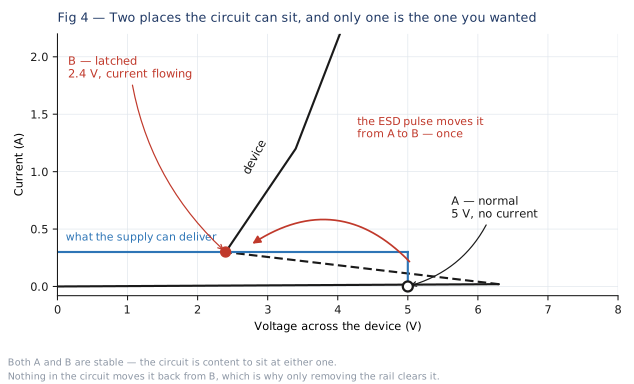
Point A is the board working: 5 V across the device, no current through it. Point B is the fault: 2.4 V, current flowing. The important word is both: each one is a place the circuit can rest indefinitely. The ESD pulse does not damage anything. It simply carries the circuit from A over to B, and once there, nothing in the circuit is pushing it back.
That is the difference between a fault that clears itself and one that does not. If the device had no fold, its conducting branch would sit entirely to the right of the rail and there would be no second crossing: only one place to sit, so no latch is possible. The fold is what creates the second home.
Two different faults share the name "latch-up"
This is worth separating carefully, because the word gets used for two different things and the fix is not the same.
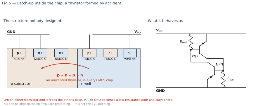
The first is latch-up inside the protected chip. Any CMOS process contains an unwanted four-layer structure: the NMOS source, the p-substrate, the n-well and the PMOS source stack up as P-N-P-N. That is a thyristor nobody designed and nobody wants. It behaves as two bipolar transistors wired so each one feeds the other's base. Normally both sit off and leak a few nanoamps. But if something injects enough current into one of them, it turns the other on, which turns the first one on harder, and the pair latches into a low-resistance path from VDD straight to ground. The transient that started it is long gone; the supply keeps it there.
The second is the protection device itself latching, the failure in this note. Nothing inside the controller misbehaved. The TVS folded back to its holding voltage and the rail was high enough to keep it there.
On the bench the two look almost identical: the rail sags to some odd fixed value, current is far too high, something is warm, and a power cycle clears it. The difference is which part is holding the current. If the protection device is the one getting hot, it is the device. If the controller is the one getting hot and the protection device is cold, the latch is inside the chip. Lifting one end of the protection device and repeating the test settles it in a minute.
What actually triggers it
Either kind needs something to inject the first burst of current. In practice:
- A transient on the port. ESD, a surge, hot-plugging a cable, or the cable's own stored charge dumping into the connector. This is the common one, and it is exactly what a USB Type-C port sees every day, because it is designed to be plugged and unplugged while live.
- The rail coming up too fast. A supply that rises quickly, or overshoots at power-on, can push enough displacement current through the parasitic structure to trigger it before the board has even started working.
- A heavy load moving the rails around. If a large current step drags the supply down or lifts the local ground, the voltage between different parts of the chip shifts, and that shift can forward-bias a junction that is supposed to stay off.
- Choosing a protection part whose holding voltage sits under the rail. This one only causes the second kind, and unlike the other three it is not bad luck. It is a selection decision, made months earlier, at a desk.
The first three are conditions you manage. The last one you simply avoid, and it costs nothing to avoid, which is what makes it the frustrating one to find in a finished product.
What it does to the board
Latch-up is not a single event, it is a state the board is stuck in. The damage builds up in stages, and how far it gets depends on how long the supply is left on and how much current it can deliver.
- The rail collapses to the holding voltage. Not to zero, but to whatever value the latched device sits at. On the board in this note, 5 V became 2.4 V. Every chip on that rail is now running below its minimum supply voltage.
- Communication stops or corrupts. The port goes dead, or worse, intermittently wrong. On a data line the same fault shows as errors and retries rather than a clean failure, which is much harder to trace.
- The current keeps rising as things heat. A latched path has low resistance, and the supply will deliver whatever its own limit allows. If the supply has a current limit, it fights the latch and both parts get hot. If it does not, the current is bounded only by the board.
- Something fails from EOS. Electrical overstress, not ESD, a slow thermal death rather than a fast one. Usually the latched device dies short. Sometimes a bond wire opens. Sometimes the chip behind it goes first.
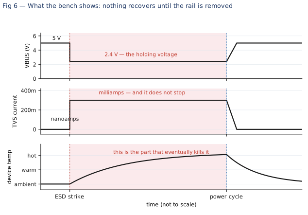
The last stage is the reason this failure keeps repeating across products. Once heat has destroyed the protection device, the evidence of the latch is gone. What arrives at the failure analysis bench is a shorted TVS on a board that failed an ESD test, which reads exactly like a part that was too weak. So the next revision fits a bigger device with a higher surge rating and, very often, the same holding voltage. The board fails the same way, and now it has more capacitance on the data lines as well.
If you take one diagnostic habit from this note, take this one: a protection device that recovers after a power cycle was never too weak. Check the holding voltage before you order a stronger part.
The trap in "lowest clamping voltage"
Here is the uncomfortable part. Snapback devices have low clamping voltages because they fold back. The fold is the feature. So when you sort a distributor's list by clamping voltage and take the best number, you are quietly selecting for devices with the lowest holding voltages, the ones most likely to latch on a powered rail.
The most attractive number on the datasheet is the one that creates the risk.
The fix
There are two valid answers, and which one you use depends on the net.
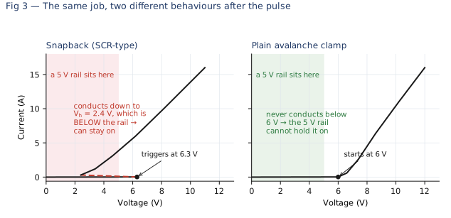
- Keep snapback, but check the numbers. The rule is simple: Vh must be higher than the maximum voltage the rail can reach, including tolerance and any overshoot. If the rail can never hold the device at or above Vh, it cannot latch.
- Use a device that does not fold back. A plain avalanche clamp has no fold. It conducts only above its breakdown voltage, so a 5 V rail simply cannot keep it on. You give up a little clamping performance and you remove the failure mode entirely.
On the board above, the second option was the right one. VBUS is a permanently powered rail, and nobody wants a protection device whose correct operation depends on the supply tolerance.
Why some devices fold back at all
It is fair to ask why anyone would build a protection device that can be held on. The answer is that the fold is not a defect. It is the whole reason those parts clamp so well. Protection devices come in three broad constructions, and the shape of the fold is what separates them.
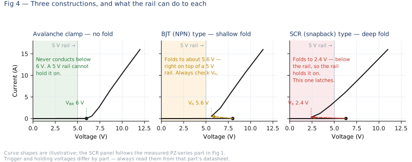
- The avalanche clamp. A diode junction that starts conducting above its breakdown voltage and keeps rising from there. No fold, so there is no holding voltage to check and no way for a rail below its breakdown voltage to keep it on. The price is that the voltage across it climbs as the current climbs, so clamping at high current is the weakest of the three.
- The BJT type. A bipolar transistor triggered by avalanche at its collector. Once conducting, transistor action holds the voltage down, so it folds, but only modestly. These sit in the awkward middle: the fold is real, and the holding voltage often lands close to common rail voltages. This is the group where people get caught, because the datasheet does not look dramatic enough to prompt the check.
- The SCR type. A deliberate four-layer thyristor, the same structure that is a parasitic accident inside a CMOS chip, here built on purpose and controlled. Both halves latch each other on, so the voltage collapses hard. That gives the lowest clamping voltage of the three and it does it in a small die, which means low capacitance. It is the best protection per square micron available, and it is the one that will sit there conducting if the rail lets it.
So the ranking that matters is not "which is best". Deeper fold means better clamping, smaller die and lower capacitance, and a higher chance the rail can hold it on. You are choosing where on that trade you want to sit, and the answer depends entirely on whether the net carries DC power.
How to catch this from the datasheet
Before a protection part goes on a powered net, three checks:
- Look for a holding voltage. If the datasheet lists Vh, compare it against your maximum rail voltage. If Vh is lower, that part can latch on that net.
- Look at the I-V or TLP curve. If the curve bends backwards, it is a snapback device, whatever the marketing text calls it. If it rises straight, it is not.
- Check whether the vendor tells you at all. Some do not publish a holding voltage. If it is missing on a part you intend to put across a live rail, ask for it, or choose a part that publishes it.
One thing not to rely on: the part number. A prefix is a family name, not a guarantee of the conduction mechanism, and across the industry, our own catalogue included, one family can contain both types. The three checks above are what settle it. If you would rather not work through a whole BOM of them, send us the part numbers sitting on your powered rails and we will check the holding voltages against your rail voltages for you.
Snapback is not a bad device
It would be easy to finish here with "avoid snapback", and that would be wrong. On a high-speed data line, snapback is often the better choice: it gives a lower clamping voltage and it does it with very little capacitance, which is exactly what a multi-gigabit lane needs. And a data line carries no DC supply, so there is nothing available to hold the device on after the pulse.
The same device that is an excellent choice on a data line is a liability across a power rail. It was never a bad part. It was a good part on the wrong net.
The short version
- A protection device that recovers after a power cycle was latched, not damaged.
- Two faults share the name: the parasitic thyristor inside the chip, and the protection device holding itself on. Whichever part is getting hot is the one that latched.
- Snapback devices fold back to a holding voltage. If the rail sits above it, they stay on.
- Compare Vh against your maximum rail voltage before you compare clamping voltages.
- Snapback belongs on unpowered data lines; use a plain clamp across live rails.